First I want to say this. The Super Scope 6 cartridge I bought didn't work. I went back to the store where the person who sold me the game hooked it up on a TV and agreed that it didn't work. He then proceeded to blowing into the game cartridge after which it did work. So that was fun. I've ordered more cheap cartridges as well as the game bit tools needed to open the cartridges/console.
My first project regarding the SNES it to make a ROM extractor. When I write “my project” or “I will need to” that is what I'm referring to! In this blog post I will not think at all about extension chips but rather focus on the “interface” between the SNES and the cartridge for non-extended games. I'm primarily interested in the PAL-version for now (in case they differ).
By visual inspection on a cartridge (PAL-SCN-Zelda), there seems to be 23 pins on the front side and 23 pins on the backside of the connector on the cartridge. In total 46 pins that may each have a role. Some of these will provide a current to power the chips in cartridge and other will be used for communication.
A video on How to Clean/Repair Super Nintendo (SNES) Games doesn't tell much but shows how a cartridge looks on the inside. This is an american cartridge and we can see that in addition to the 23 pins it has two additional pairs of 4 pins on the sides. Summing it up we have 62 pins in total. Why does that game have more than the one I checked earlier? The PAL SNES have 62 pins in the console so it seems that some games may use more pins, probably for extension chips in later games. The game StarFox shown in the video uses the SuperFX extension chip.
I found a SNES Cartridge pinout that shows what 48 out of the 62 pins do. Their scheme for the pin layout is as follows (the // means that they've cut out a portion from the visual table!):
+-------------------------------//----------------------------+ | 32 33 34 35 | 36 37 38 39 40 //53 55 56 57 58 | 59 60 61 62 | | 01 02 03 04 | 05 06 07 08 09// 22 24 25 26 27 | 28 29 30 31 | +----------------------------//-------------------------------+
If we look at the voltages it expects we have:
5: GND 27: +5 VDC 36: GND 58: +5 VDC
The ground and the potential are located on opposite sides of each other, close to each other.
Furthermore there are 24 pins to describe an adress, which seems right since the SNES uses 24-bit pointers/adresses (8-bit for bank and then 16-bit for offset in bank). Often the execution of an opcode uses a bank stored in a register on the SNES CPU, but it seems that the cartridge always get the full 24-bit adress.
There are a few more pins that are interesting.
23: Read 26: RAM enable 49: ROM enable 54: Write
Since the cartridge supports both reading (from ROM and SRAM (save games)) and writing (to SRAM) the cartridge needs to now what it should do. RAM/ROM enable probably indicate where the cartridge should read/write.
Then there are 8 pins labelled “Data”. 8 pin equals one byte. I suspect it is where the result of a ROM/RAM read ends up, or the thing to be written to RAM. If it both acts as read result and write then they might be bidirectional. That is, depending on bit 54 (and 23?) they either acts as inputs or outputs.
That leaves leaves 4 pins labelled “CIC”, 1 pin labelled “IRQ” as well as the unlabelled extra pins that makes it 62 instead of 48. The CIC is related to the lock-out chip. Rumor has it that the lockout chip needs a current, not sure if that is applied at one of the CIC-pins or if one of the +5VDC are inteded for that. Looking inside a cartridge would perhaps tell me where the +5VDC are going.
More information comes here! I knew there was more data on the internet but I'd like the interpret what I found first to draw my own conclusions! It details all the 62 pins.
While the two documents uses the same pin ordering, they do contain one contradiction regarding pin 26. The first one says “RAM Enable” and the second one says “RESET”.
I've talked to ikari_01 on ircnet #snesdev and he told me the following:
- The data pins generate 0V to indicate zero and +5V to indicate one.
- For ROM-extraction the CIC (lockout chip) can be ignored for most cartridges! It only acts to unlock the console, not the cartridge. The extension are games with certain extension chips (SA1 and SDD1). See list of games here.
- shiftplusone on freenode #raspberrypi-dev suggested running the cartridge on +3.3V instead of +5V. ikari_01 said that it would probably work for most games. I will talk later on why this.
If I get the electronics sorted out it seems quite easy to get the data out. Feed some pins with 0 or 1, iterate over all adresses and then read out the data values. One problem I haven't found a solution to yet is how they sync. When do I write/read? I'm sure it is once a cycle or something like that, but when does the cycle start? It seems like the SNES should tell the cartridge somehow, either once at reset or at every cycle. There are some pins that I don't know what they do (like CPU_CLOCK) and I'm sure I'll figure it out later.
Images inside a cartridge
My game bits arrived! Here are some images from inside the Super Scope 6:
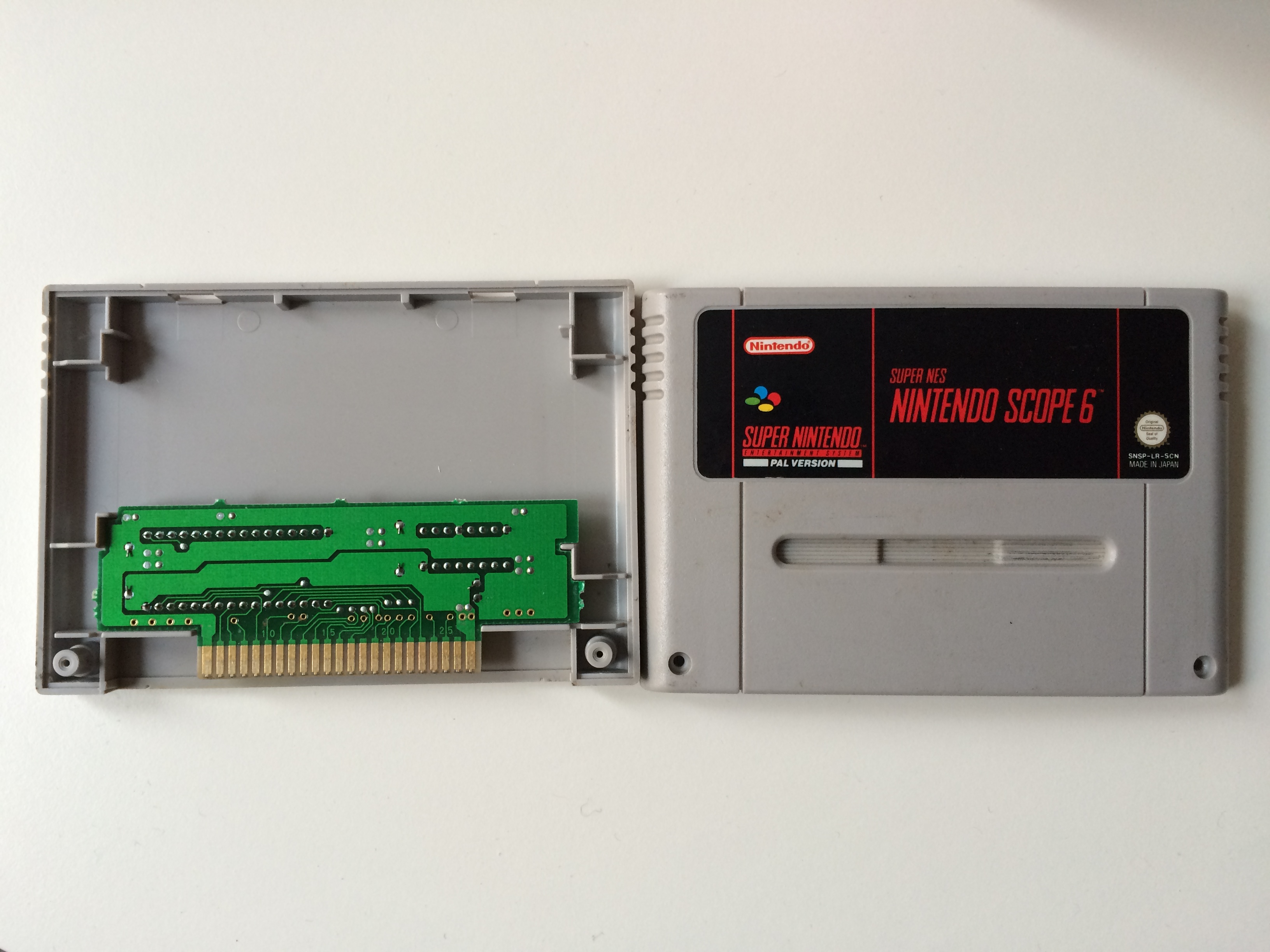
Here is a closeup. Mostly air!
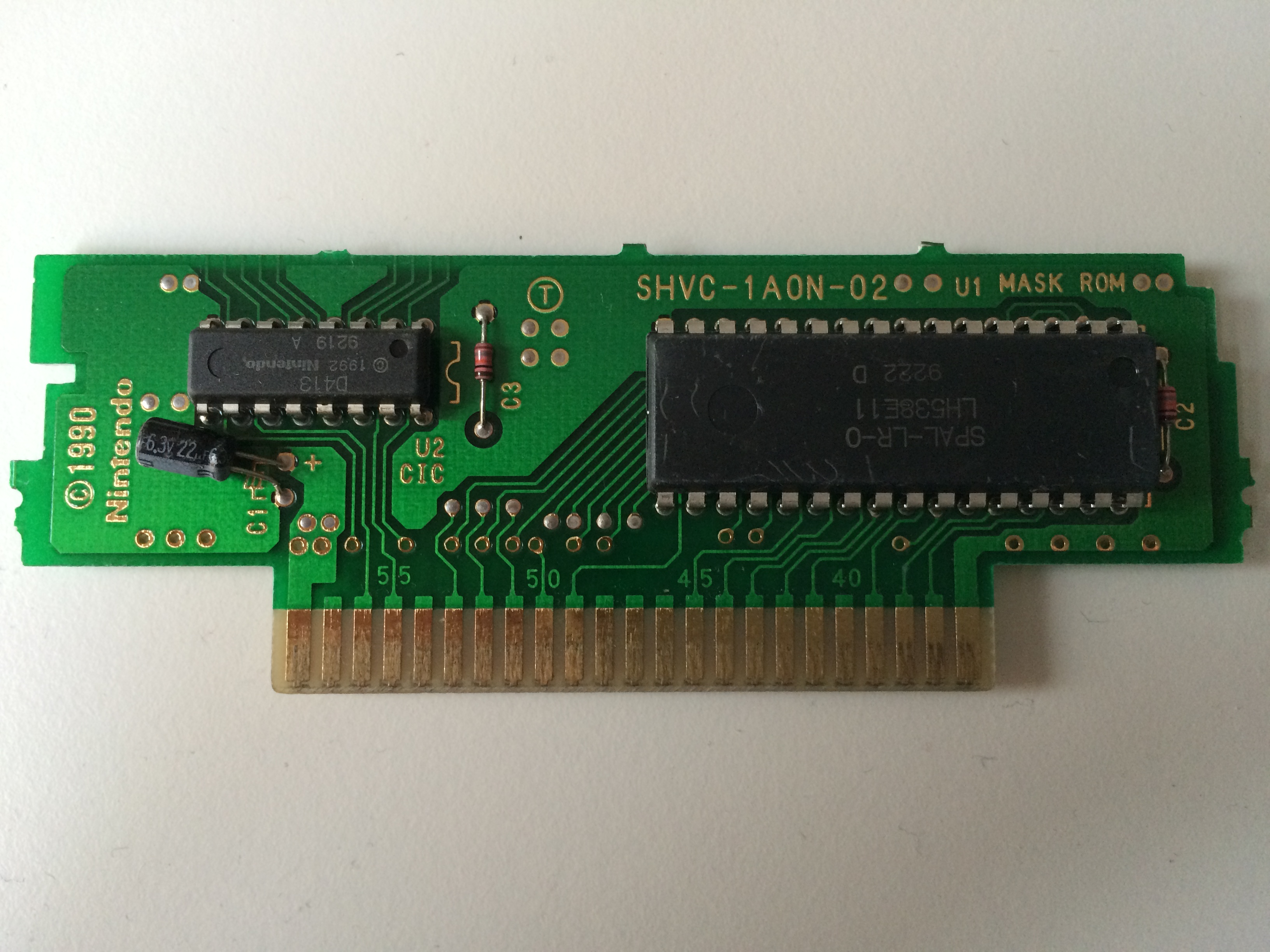
Here is the front side of the PCB. It has two IC as well as some other junk. The IC named D413 is the CIC (lockout chip) used for PAL cartridges. The other one (the big one) probably contain the ROM and logic.
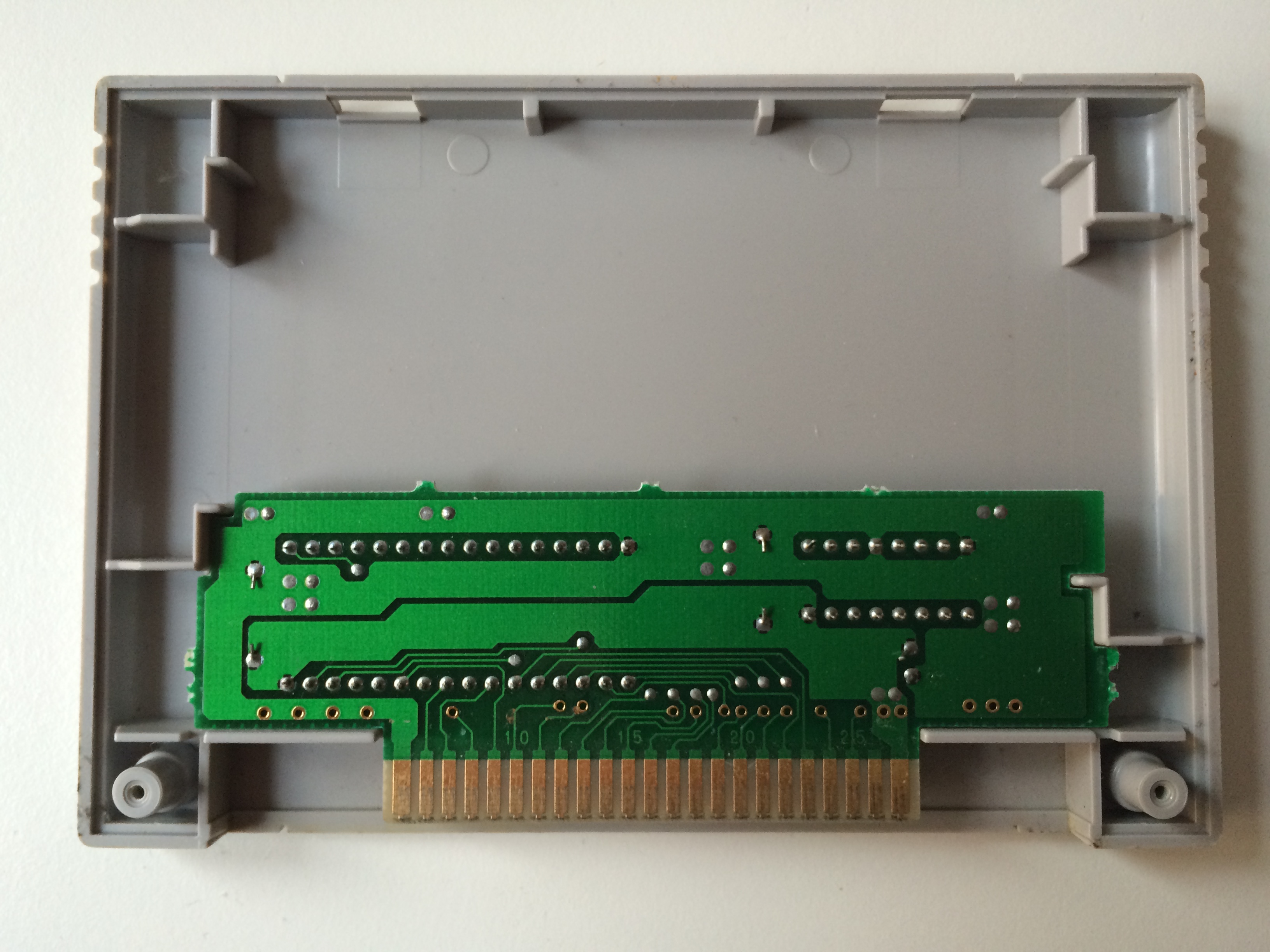
Same image but upside down, for people with their heads upside down:
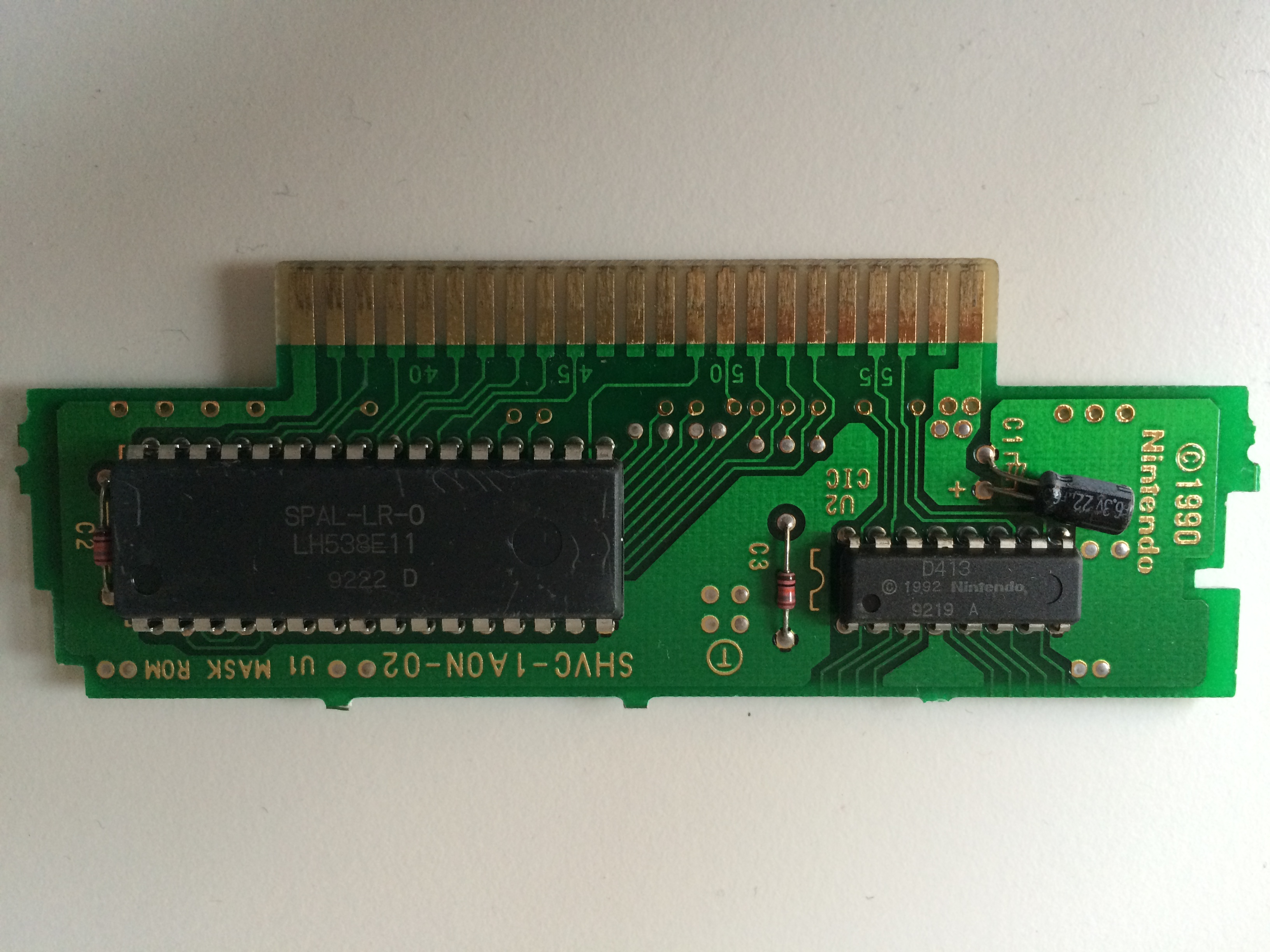
And here is the backside:
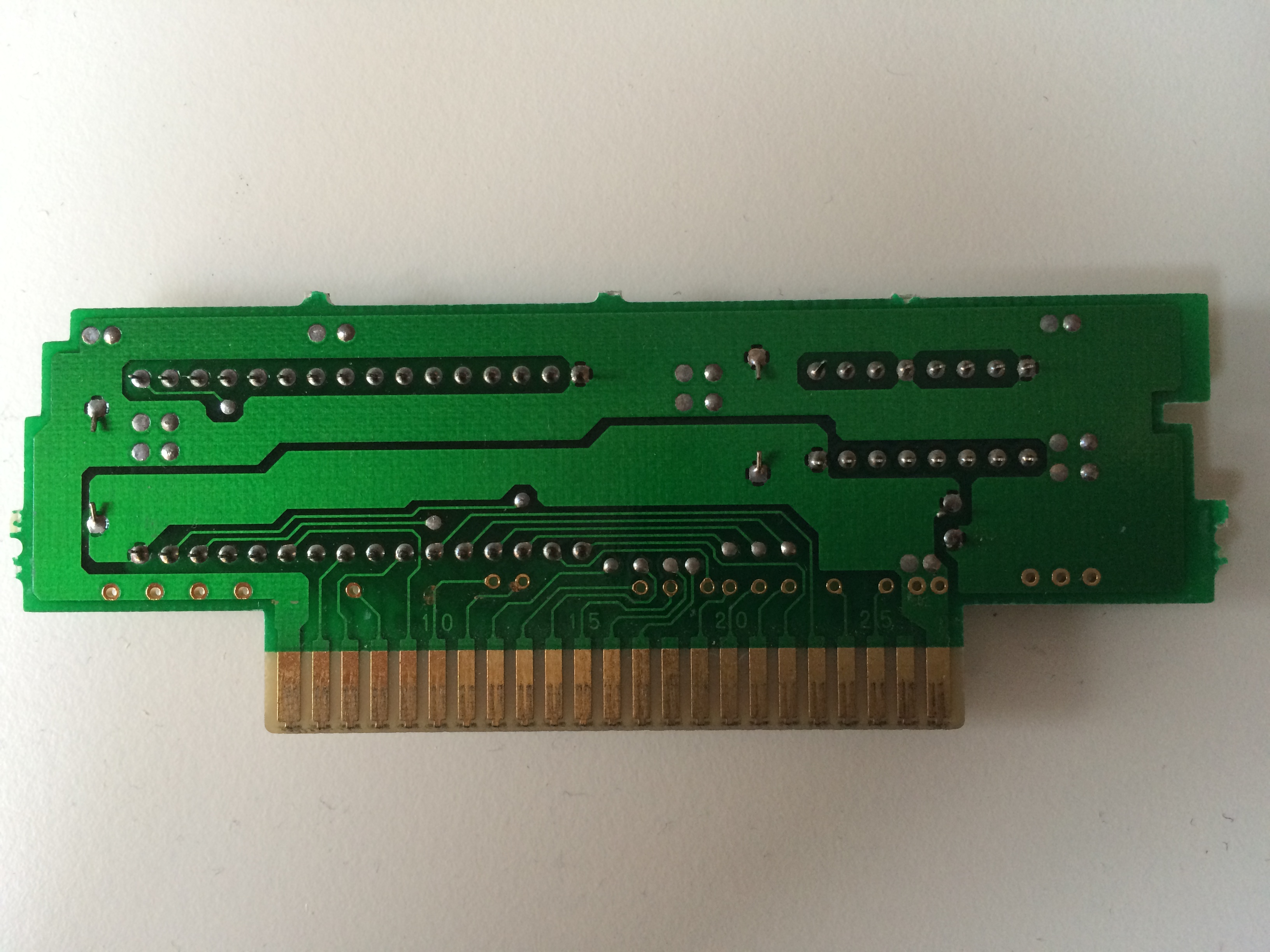
It would be interesting to figure out if the CIC is totally isolated from the rest of the PCB so that I can ignore those pins. Also it would be interesting to see if both +5VDC/GND are used or if one pair is for the CIC.
Connecting a SNES cartridge to a breadboard
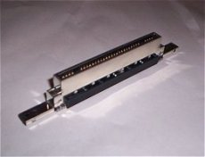
It seems one can buy a new (or used) 62-Pin Connector. There are two versions, one that you need to solder onto your SNES yourself and one that is more plug-n-play.
Solder-version:
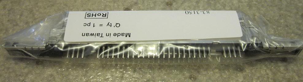
Plug-n-play-version:
This seems like the easy way out but, according to ikari_01, the pins on the official connector are 2.5mm apart, while the holes on a breadboard are 2.54mm apart. Thus I would have to force the pins into the breadboard, probably having to ignore the outermost 4 pins (for the extension chips). Also it is easier to get the plug-n-play version but that would be much harder to use since it has no pins at all. I've been thinking about getting my hands on an action replay since that would have both a 64-pin connector at the top and also would work as a cartridge to plug into the SNES if I ever need that. Two for one, cheaper than any of the 62-pin connectors I've found.
An alternative is to buy a standard edge connector, like the one used in a PCI-buss. They have pins 2.54 apart, just like the breadboard have. It has too many pins so some would have to be cut off. From the data sheets it is unclear if the pins are too wide or not, but I'll guess I'll just get some and find out. The distance between the plates where the cartridge connect would be slightly offset (by 0.04mm per plate), but the accumulated error after 22 plates would only be 0.88mm which is much smaller than the width of a single plate (more than 1mm).
One other option would be to do something myeslf. Small insulated clamps that has attached seperate wires for each hand that connects to the two plates? Maybe make a strip of plastic with several wires and attach using clothing pegs? Maybe 3d-print a plastic frame and mount wires? Alternatives are endless. But with so many pins it would require a lot of laboring.
I'll stop here, but I'll continue later!